
R&D

Contents
Display R&D (LCD/OLED)
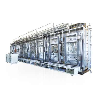
- Large-area TFT Sputter
- CF Sputter
- Thin film encapsulation
- Oxide TFT Sputter
- Oxide TFT element inspection equipment
- Semiconductor R&D
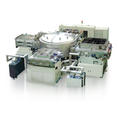
- Sputter for WLP(Wafer Level Package) and PLP(Panel Level Package)
- Energy R&D
- Isotope (Ni-63) battery
- Solid-state battery
Solar Cell R&D
- CIGS Solar Cell
- Sputter for Back Electrode (Mo), Diffusion Barrier (SiO2), CIG Precursor, Window (ITO, AZO) deposition
- NFS (Nozzle Free Se Shower) RTP for heat treatment of CIGS light absorbing layer
- ALD for deposition of dry Buffer((Zn(O,S), ZnS, Cd(Zn,S))
- MOCVD for Window(BZO) deposition
- Crystalline-Si Solar Cell
- Passivation
Other R&D
- Analytical Simulation
- Structural analysis
- Heat, Flow analysis
- Magnet, Plasma analysis
- Semiconductor
- Etching Uniformity Improvement Technology
- Particle Control Technology
- Other Industrial Deposition Equipment
- High-speed and high-efficiency deposition equipment
- Damage-free deposition equipment